ZnO Nanostructures
ZnO nanowires and related materials
Semiconductor nanowires (NWs) have been proposed as basic “building blocks” in a variety of devices in many applications, such as photonics, electronics and chemical sensing . For instance, the large surface area offered by NWs is very attractive for solar cells where high surface chemical sensitivity and efficient light trapping and absorption are needed.
ZnO offers Interesting optical, electronic and electro-mechanical properties, such as
1. Large bandgap 3.3 eV (UV)
2. Large excitonic binding energy (60meV, which means stable excitonic emission)
3. Large piezoelectricity (opportunity for MEMS devices
4. High surface reactivity (catalysis, photocatalysis, electrolytic solar cells…)
ZnO nanowires growth
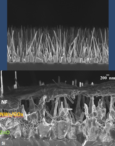
Most studies report on efforts to grow vertically aligned ZnO NW arrays on various substrates (notably on Si and saphire). An important requirement for cost-effectiveness is the possibility of growing NWs on inexpensive and transparent substrates, such as glass. In such an amorphous substrate, growth of vertically aligned ZnO NWs on a vacuum deposited SiO2 film on a Si substrate can be achieved by fabricating a thin seed ZnO layer on the SiO2 film prior to NW growth.
ZnO nanowires grown by the NANO project team on SiO2
The image above shows partially aligned, high crystallinity ZnO nanowires that grew on an amorphous SiO2substrate. The partial alignment is believed to be due to a very thin ZnO layer that grew at the SiO2 and helped seed ordered nanowire growths.
The growth system (LAFISO)
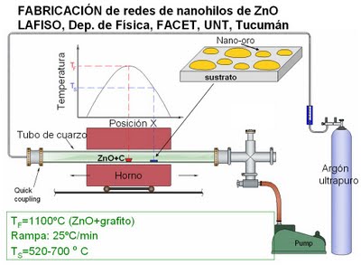
NW growths were performed at the LAFISO vapor-transport system, which was designed and set up using an existing furnace especially for this project.
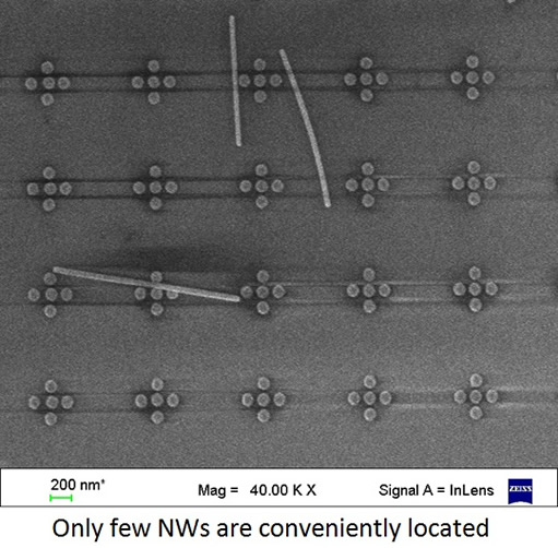
It consists of a 1 3/8 " diameter, 1 m long quartz tube placed within a 0.6 m length tubular furnace. One side of the quartz tube is seal-connected through a vacuum valve to a rotary pump while its other side to a high purity (99.999%) Ar line made of a 1/4 " diameter stainless steel tube. An alumina crucible containing ZnO and graphite powders (2:1 volume ratio) was placed inside the quartz tube at a position corresponding to the furnace center. Pairs of Si (100) and SiO2/Si substrate pieces were placed parallel to the tube axis facing upwards at two different distances downstream the tube (16 and 19 cm from the furnace center), which resulted in two different substrate temperatures due to the natural temperature gradient profile along the tube.
The image above shows typical process variables used in the fabrications.
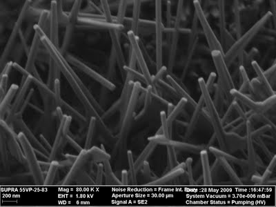
ZnO nanowires networks
An interesting and potentially useful assembly is in the form of ramdom networks of interconnected NWs on insulating substrates. Direct growth of randomly-oriented ZnO NW networks on thermal SiO2 layers on Si using the metal catalysis method. Has been achieved. The electrical properties of the NW networks can be easily tested right on the insulating SiO2/Si growth substrates and exhibit macroscopic conduction and photoconduction with potential sensor, photovoltaic and other optoelectronic applications
From D. Comedi et al., J. Alloys and Compounds 495, 439-442 (2010)
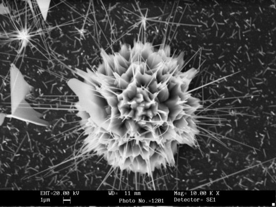
ZnO nanoflowers
Marvelous ZnO structures grow as a result of combined 3D, 2D and 1D growth. This structure was obtained accidentally in our system in Tucuman on top of a Si substrate containing Si nanowires (which can be seen as tiny fingers at the back) grown by our Collaborators at the Polytechnique University of Madrid.
Substrate distance from vapour source sets ZnO nanowire's size and luminescence
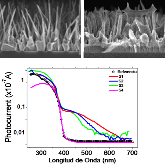
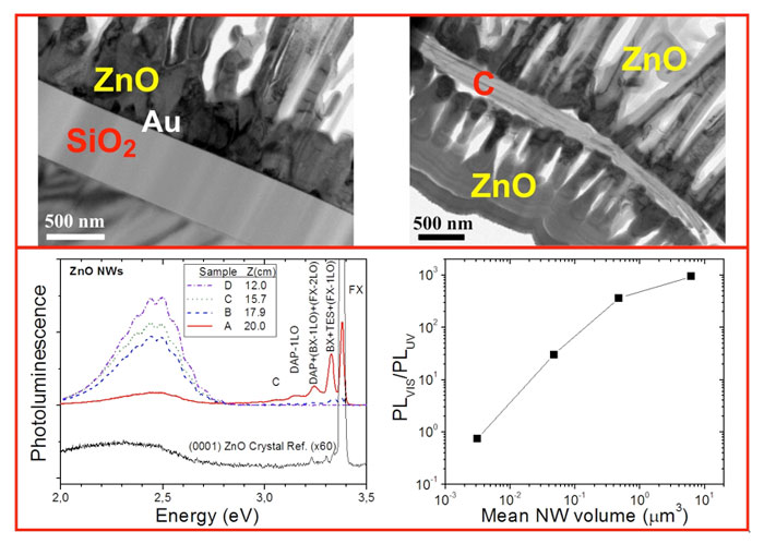 ZnO NWs were grown via vapour transport deposition (VTD) using the system shown above. When such a transport is performed in advection (as opposed to diffusion) conditions, vertically aligned ZnO NWs are obtained on the amorphous SiO2 substrates that had been previously coated with Au nanoclusters. The key point is that, in contrast to most cases discussed in the literature, NW growth here does not proceed by the so-called vapour-liquid-solid mechanism. Instead, the synthesis involves a self-deposited ZnO wetting layer on top of the Au nanoclusters, which is then followed by a vapour-solid growth of the ZnO NWs on it (top-left figure). As a byproduct, micrometric patches of distinct NW morphology evident on the substrates were analyzed and identified as aligned ZnO NWs that had grown on carbon flakes (top-right figure). These micrometric flakes, which apparently were just graphite particles dragged by the gas flux from the ZnO+graphite source that had landed on the SiO2 substrates, are able to promote NW growth without the presence of any metal catalyst or ZnO wetting layer on their surface. This is a quite interesting result because the use of ZnO NWs as "field-enhancing nanoarresters" has been proposed as ways of outperforming current C-based electrodes in various field-emission applications.
Increasing the substrate to vapour source distance (Z) by just 8 cm, the growth mode can be changed smoothly from one leading to complex, porous networks of interconnected NWs with interesting sensor applications, to another leading to well separated, highly UV luminescent NWs, strikingly showing the potential tailoring capability of this technique for many photonic applications. This can be seen in the bottom-left figure, where a strong increase of the relative UV luminescence intensity occurs. The bottom-right figure shows that, in addition, a three orders of magnitude decrease in NW volume is observed.
From N. Vega et al. in Nanotechnology (http://dx.doi.org/10.1088/0957-4484/23/27/275602)
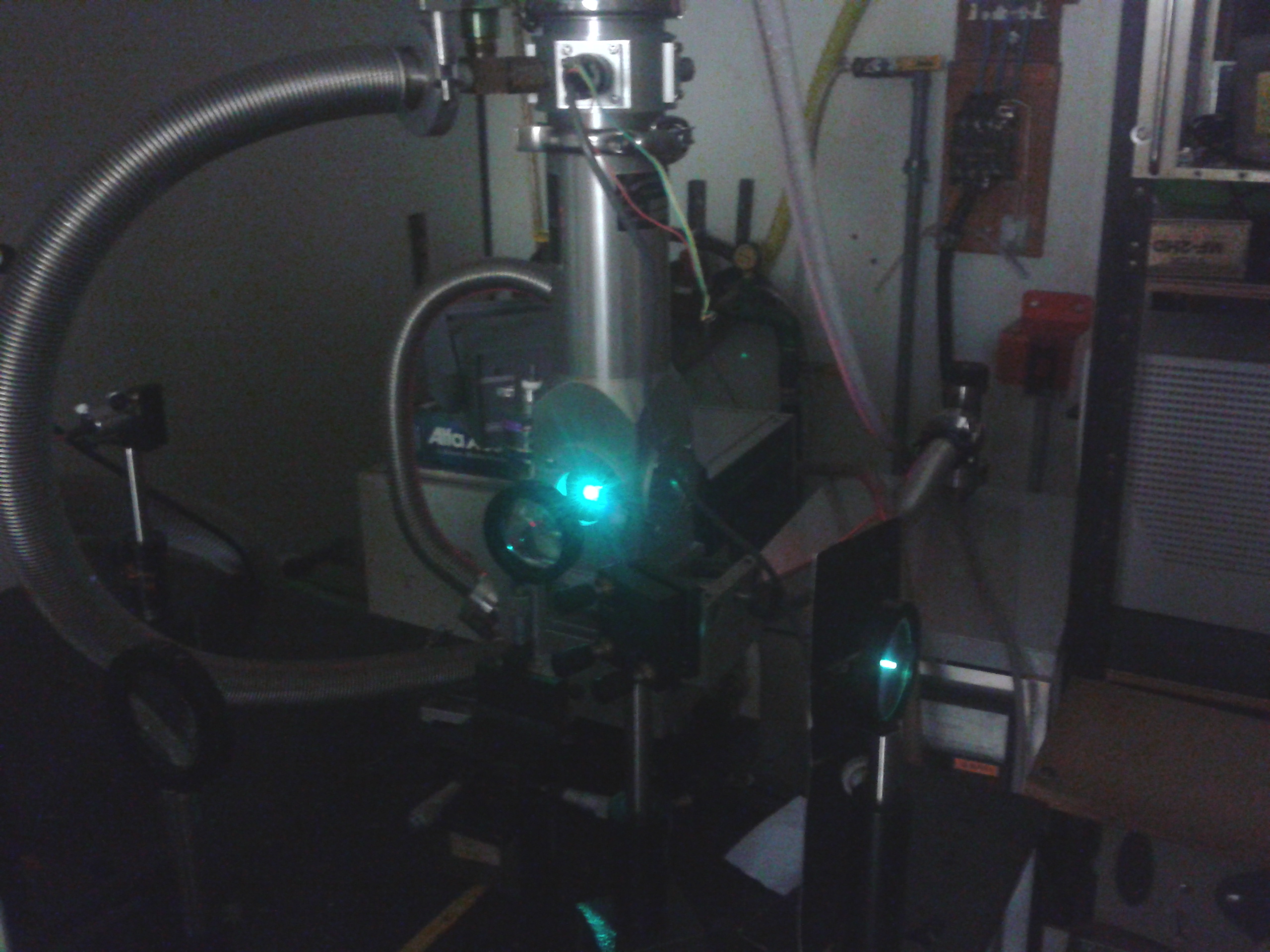
Luminescence Studies - Photoluminescence of ZnO nanostructures: Surface correlation and Fabry-Perot modes
The picture shows the bright green photoluminescence from ZnO nanowires excited by a HeCd laser (325 nm).
- Surface correlated photoluminescence of ZnO nanostructures
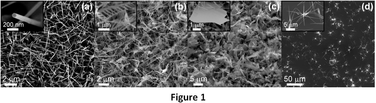
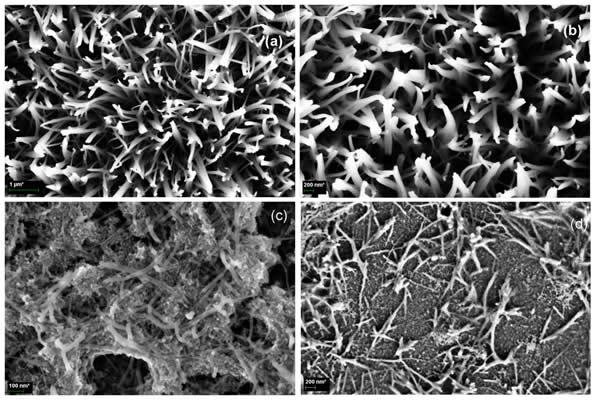
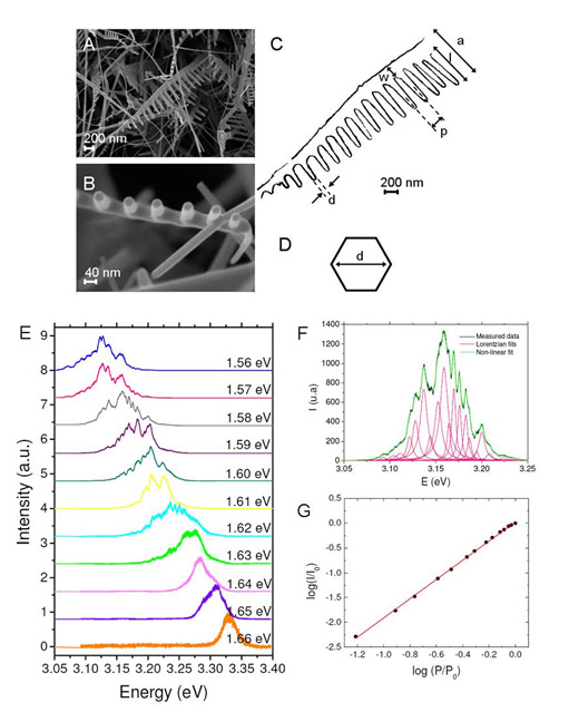
Hierarchical ZnO nanostructures were fabricated using the growth system shown above. On Au nanocluster covered c-Si and fused and thermal silica (type I, II and III substrates respectively), ZnO nanowires (NWs) grew [Fig. 1(a)]. However, the growth pattern changed to nanocombs (NCs) and nanosheets (NSs) [Figs. 1 (b) and (c) respectively] when decreasing the O2 to local Zn partial pressure ratio (i.e. diminishing the amount of oxygen respect to Zn over the substrate), via altering the O2 flux or the vapour source - substrate distance. ZnO nanohedgehogs (NHs) [Fig. 1(d)], which are composed by a micrometric core from which nanowires grow radially, were found on bare c-Si (type IV substrate). These nanostructures do not grow from the substrate and presumably had landed there after being dragged by the Ar+O2 flux.
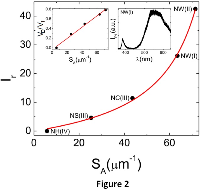 A typical photoluminescence spectrum (NWs on type I substrate) is shown in the rightmost inset of Fig. 2. The UV peak is the free exciton related emission while the intense visible band centered in the green is defect related luminescence, often attributed to O deficiencies such as O vacancies or Zn interstitials. The main graph of Fig. 2 shows the ratio Ir = IVIS/IUV (integrated visible photoluminescence intensity over the corresponding integrated UV intensity) as a function of the specific surface area SA (surface area over volume) for all types of nanoobjects. A remarkable non-linear correlation was found. Generalizing a model applied in the literature only to NWs, we found that the effective volume of defects respect to the total volume in a nanostructure (VD/VT) increases linearly with SA (left inset of Fig. 2). This indicates that visible luminescence comes from surface states, and that the density of those states is approximately the same for all types of nanostructures. O deficiency defects at surfaces are then responsible for the observed morphology changes, one to two-dimensional growth transition (from NWs to NCs and NSs), and corresponding luminescence.
From G. Grinblat et al. in Applied Physics Letter ( http://dx.doi.org/10.1063/1.4724195)
- Fabry Perot modes in ZnO nanocombs
The UV region of the photoluminescence spectra of ZnO nanostructures contains various peaks whose different patterns depend on the type of nanostructure and its orientation with respect to the incident polarization, and it is found to be dominated by free exciton emission (FX) and their phonon replicas. For the nanocomb (NC), however, Fabry-Perot modes originating from optical multiple reflections within the NC teeth are demonstrated. Fig. 3(a) shows the spectrum at three different locations of the ZnO NCs sample [SEM picture in Fig. 1(b)]. Since these nanostructures are randomly orientated over the substrate and the size of the polarized excitation spot (10 micron^2) is approximately the size of a single NC, the measurement is sensible to the region of study. The phonon replicas will be more visible when the NC teeth are aligned with the incident polarization. As it can be seen from the figure, different peaks appear at different sample locations.
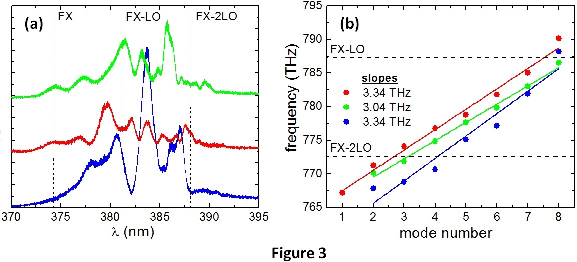
Besides the FX emission and phonon replicas, we observe modes with smaller spacing that correspond to Fabry-Perot optical modes. This is demonstrated in Fig. 3(b), which shows a linear behavior for the frequency of the maxima as a function of the mode order for the three spectra in Fig. 3(a). The length of the resonators, which are the NC teeth, results to be d = 1.5 ?m in accordance with the lengths measured at the SEM image. In order to establish stationary modes in a Fabry-Perot resonator, both ends of the cavity should be parallel and high optical quality reflectors. In our system, besides, all resonating cavities for a single NC have similar lengths and orientations, so Fabry-Perot modes are still detectable for the whole nanostructure. This proves the high quality of the nanostructure and promising applications in nanolasers.
From G. Grinblat et al. in ECS Transactions ( http://dx.doi.org/10.1149/1.3700411)
Impedance Spectroscopy of Nanowire Solar Cells
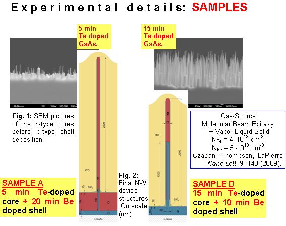
Typically, PV device performance is assessed through DC current-voltage characteristic measurements. However, a much more complete device characterization can be achieved by studying the frequency dispersion of electrical properties. In this work, we present an impedance spectroscopy study of core-shell GaAs NW p-n junction structures fabricated by gas source molecular beam epitaxy (GS-MBE) for PV applications where Te has been used as the n-type dopant. The use of Te instead of the more common Si as the n-dopant derives from the amphoteric behavior that Si may exhibit in GaAs NWs.
Impedance spectroscopy studies in the 10-107 Hz and -40, +40 V frequency and bias ranges can be performed at the Nanomaterials and Dielectric Properties of Matter Laboratory (LNPD), at the Physics Department, FACET-UNT.
Impedance Data
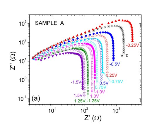
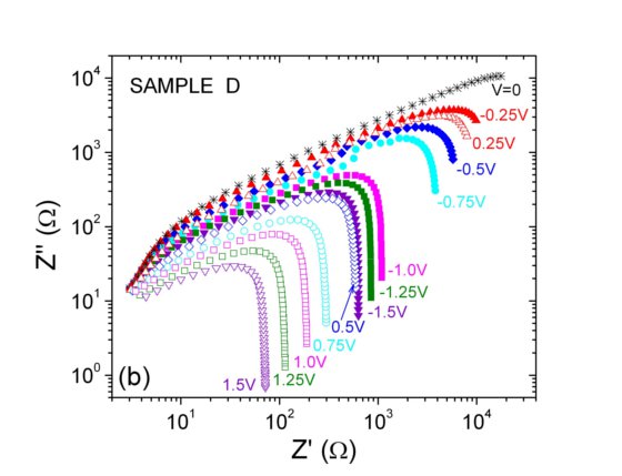
The impedance data in the complex plane show strong differences which are related to the different n-p spatial distributions of samples A and D above.
The results below show that, under proper fabrication conditions, the experimental impedance follows the behaviour expected for a p-n junction but, nevertheless, they emphasize the role of surface traps in the transport and recombination mechanisms and interface space-charge regions in the studied devices.
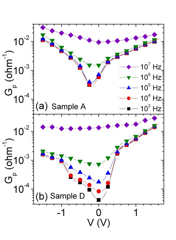
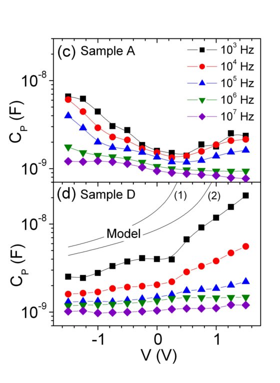
Conductance and Capacitance as extracted from the impedance data of Figs. 5 and 6, for samples A and D. The core-shell capacitance for sample D in Fig. 8(b) is modelled by a coaxial cylindrical charge sheet capacitor for (1) Vbi=0.65 V and (2) Vbi= 1.2 V, where Vbi is the built=in potential at the p-n junction.
From J. Caram et al. in Nanotechnology (http://iopscience.iop.org/0957-4484/21/13/134007/?rss=2.0
Luminescent Si nanostructures
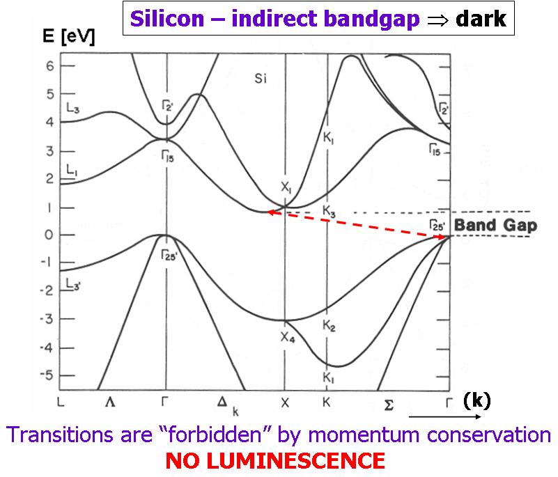 Bulk silicon (Si) is the basis of our telecommunications and computational technology. The highly developed Si technology has enabled the fabrication of excellent transistors and photodetectors and, by combining Si with its natural oxide—silicon dioxide (SiO2) —outperforming waveguides have been designed and produced as well. However, Si possesses an indirect band gap and therefore it does not exhibit room-temperature luminescence. This has been the major obstacle to completion of an all-Si photonic circuit. Although most of the Si-based computing and communication functions have already been developed, a practical Si light source is still lacking. That is why huge efforts have been directed in recent years towards making Si an efficient, reliable luminescent material.
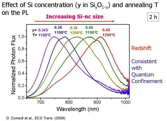
Fortunately, when silicon is prepared in special nanoscopic forms, such as Si nanoparticles or nanocrystals (Si-nc), bright luminescence at room-temperature eventually occurs. The “particle-in-a-box” or “quantum confi nement” concept has been used to rationalize the effect. According to Heisenberg’s uncertainty principle, the confi nement of an electron to a nanometer space region blurs out its momentum, thus enabling “quasi-direct” luminescent transitions to occur even across an indirect bandgap. Furthermore, the energy released in these transitions, which determines the wavelength of the emitted light, should scale with the “box” size, namely, with the Si-nc characteristic size.
Si nanoparticles embedded in a SiO2 matrix
An interesting approach to prepare Si-ncs, which is fully compatible with standard Si technology, involves thermal promotion of Si-nc formation within a SiO2 layer. This can be accomplished by (a) fabricating a Si “suboxide” thin fi lm, i.e., a Si oxide where the Si concentration is tailored to be slightly larger than that of SiO2 and (2) promoting the formation of the stable SiO2 phase by a high-temperature heat treatment of the suboxide fi lm and the precipitation of Si nanoclusters withn the SiO2 matrix.
From D. Comedi et al
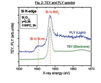
Synchrotron radiation excited luminescence and total electron yield from Si nanoparticles embedded in SiO2as a function of the excitation energy. (in collaboration with Prof. P. Mascher and coworkers from CEDT, McMaster University).
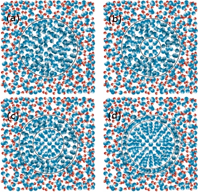
Schematic description of structural model deduced from the XRD, Raman, ESR and XAS data: (a) the as-grown oxide exhibits very poor medium range order, strong chemical disorder and embedded fully amorphous Si nanoclusters; (b) after annealing at Ta > 900ºC the oxide exhibits greatly improved chemical order and crystalline nuclei are spontaneously formed within the amorphous Si clusters; (c,d): for Ta = 1000ºC and 1100ºC, the crystalline core grows at the expense of the thinning amorphous Si shell, while the oxide's medium range order is greatly improved.
From L. J. Borrero-González, L. A. O. Nunes, F. E. G. Guimarães, J. Wojcik, P. Mascher, A. M. Gennaro, M. Tirado, D. Comedi, amorphous to crystalline silicon nanoclusters: structural effects on exciton properties, J. Phys.: Condens. Matter 23, 505302 (2011). (http://iopscience.iop.org/0953-8984/23/50/505302).
See also: Growing Si Nanocrystals within a-Si Nanoclusters Embedded in a-SiO2: Evolution of Photoluminescence (Invited), ECS Transactions 45 (5) 11-19 (2012) 10.1149/1.3700405. (http://dx.doi.org/10.1149/1.3700405).
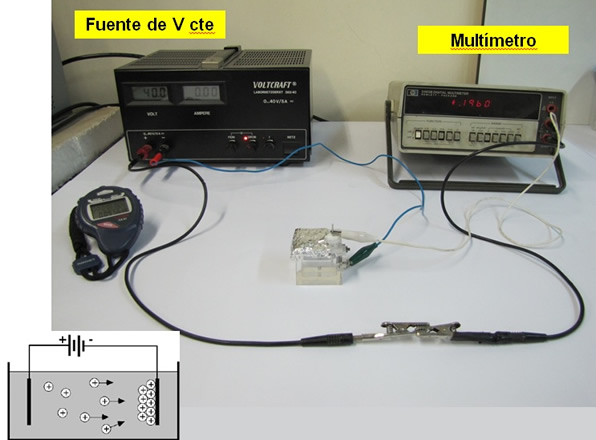
Electrophoretic Deposition
Nanophotonics and Nanoplasmonics
Biosensors and organic/inorganic hybrid interfaces
Photosensitized ZnO Nanowire electrodes for Graetzel Solar Cells